- 您现在的位置:买卖IC网 > Sheet目录2009 > MAX5150BCEE+ (Maxim Integrated Products)IC DAC 13BIT DUAL LP SER 16-QSOP
MAX5150/MAX5151
Bipolar Output
The MAX5150/MAX5151 can be configured for a bipo-
lar output, as shown in Figure 11. The output voltage is
given by the equation (OS_ = AGND):
VOUT = VREF [((2 x NB) / 8192) - 1]
where NB represents the numeric value of the DAC’s
binary input code. Table 3 shows digital codes and the
corresponding output voltage for Figure 11’s circuit.
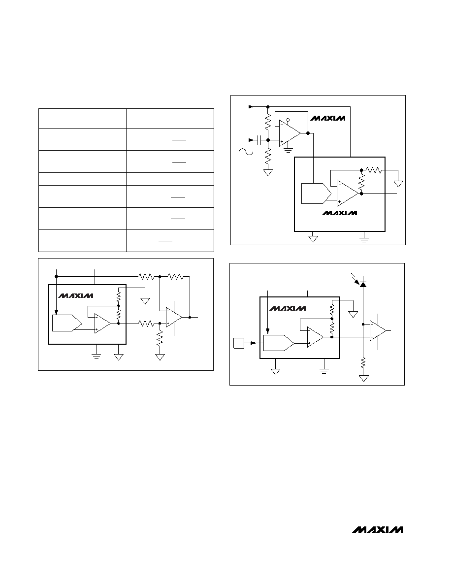
Using an AC Reference
In applications where the reference has an AC signal
component, the MAX5150/MAX5151 have multiplying
capabilities within the reference input voltage range
specifications. Figure 12 shows a technique for apply-
ing a sinusoidal input to REF_, where the AC signal is
offset before being applied to REF.
Harmonic Distortion and Noise
The total harmonic distortion plus noise (THD+N) is typ-
ically less than -78dB at full scale with a 1Vp-p input
swing at 5kHz. The typical -3dB frequency is 300kHz
for both devices, as shown in the
Typical Operating
Characteristics.
Digital Calibration and
Threshold Selection
Figure 13 shows the MAX5150/MAX5151 in a digital
calibration application. With a bright light value applied
to the photodiode (on), the DAC is digitally ramped until
it trips the comparator. The microprocessor stores this
“high” calibration value. Repeat the process with a
dim light (off) to obtain the dark current calibration.
Low-Power, Dual, 13-Bit Voltage-Output DACs
with Serial Interface
14
______________________________________________________________________________________
Table 3. Bipolar Code Table
ANALOG OUTPUT
11111
1111
10000
0000
0001
DAC CONTENTS
MSB
LSB
10000
0000
0V
01111
1111
00000
0000
00000
0000
0001
+V
4095
4096
REF
+V
1
4096
REF
-V
1
4096
REF
-V
4095
4096
REF
-V
4096
- V
REF
=
AGND
DGND
R
TOLERANCES: 10k
± 0.1%
MAX5150
MAX5151
DAC _
REF_
OS_
OUT_
10k
V-
V+
VDD
VOUT
+5V/+3V
Figure 11. Bipolar Output Circuit
DAC_
OUT
MAX5150
MAX5151
10k
26k
OS_
REF
R
VDD
GND
AGND
+5V/
+3V
AC
REFERENCE
INPUT
500mVp-p
MAX495
+5V/+3V
Figure 12. AC Reference Input Circuit
AGND
DIN
P
DGND
MAX5150
MAX5151
DAC _
REF_
OS_
OUT_
R
V-
V+
PHOTODIODE
V+
VDD
VOUT
RPULLDOWN
+5V/+3V
Figure 13. Digital Calibration
发布紧急采购,3分钟左右您将得到回复。
相关PDF资料
MAX5152ACEE+
IC DAC 13BIT DUAL LP SER 16-QSOP
MAX5155ACEE+
IC DAC 12BIT DUAL LP SER 16-QSOP
MAX5176AEEE+T
IC DAC 12BIT LP SERIAL 16-QSOP
MAX5183BEEI+T
IC DAC 10BIT DUAL 40MHZ 28-QSOP
MAX5184ETG+T
IC DAC 10BIT DUAL 40MHZ 24-TQFN
MAX5186BEEI+T
IC DAC 8BIT DUAL 40MHZ 28-QSOP
MAX5190BEEG+T
IC DAC 8BIT 40MHZ 24-QSOP
MAX5191BEEI+
IC DAC 8BIT DUAL 40MHZ 28-QSOP
相关代理商/技术参数
MAX5150BCEE+T
功能描述:数模转换器- DAC 13-Bit 2Ch Precision DAC RoHS:否 制造商:Texas Instruments 转换器数量:1 DAC 输出端数量:1 转换速率:2 MSPs 分辨率:16 bit 接口类型:QSPI, SPI, Serial (3-Wire, Microwire) 稳定时间:1 us 最大工作温度:+ 85 C 安装风格:SMD/SMT 封装 / 箱体:SOIC-14 封装:Tube
MAX5150BCEE-T
功能描述:数模转换器- DAC RoHS:否 制造商:Texas Instruments 转换器数量:1 DAC 输出端数量:1 转换速率:2 MSPs 分辨率:16 bit 接口类型:QSPI, SPI, Serial (3-Wire, Microwire) 稳定时间:1 us 最大工作温度:+ 85 C 安装风格:SMD/SMT 封装 / 箱体:SOIC-14 封装:Tube
MAX5150BCPE
功能描述:数模转换器- DAC RoHS:否 制造商:Texas Instruments 转换器数量:1 DAC 输出端数量:1 转换速率:2 MSPs 分辨率:16 bit 接口类型:QSPI, SPI, Serial (3-Wire, Microwire) 稳定时间:1 us 最大工作温度:+ 85 C 安装风格:SMD/SMT 封装 / 箱体:SOIC-14 封装:Tube
MAX5150BCPE+
功能描述:数模转换器- DAC 13-Bit 2Ch Precision DAC RoHS:否 制造商:Texas Instruments 转换器数量:1 DAC 输出端数量:1 转换速率:2 MSPs 分辨率:16 bit 接口类型:QSPI, SPI, Serial (3-Wire, Microwire) 稳定时间:1 us 最大工作温度:+ 85 C 安装风格:SMD/SMT 封装 / 箱体:SOIC-14 封装:Tube
MAX5150BEEE
功能描述:数模转换器- DAC RoHS:否 制造商:Texas Instruments 转换器数量:1 DAC 输出端数量:1 转换速率:2 MSPs 分辨率:16 bit 接口类型:QSPI, SPI, Serial (3-Wire, Microwire) 稳定时间:1 us 最大工作温度:+ 85 C 安装风格:SMD/SMT 封装 / 箱体:SOIC-14 封装:Tube
MAX5150BEEE+
功能描述:数模转换器- DAC 13-Bit 2Ch Precision DAC RoHS:否 制造商:Texas Instruments 转换器数量:1 DAC 输出端数量:1 转换速率:2 MSPs 分辨率:16 bit 接口类型:QSPI, SPI, Serial (3-Wire, Microwire) 稳定时间:1 us 最大工作温度:+ 85 C 安装风格:SMD/SMT 封装 / 箱体:SOIC-14 封装:Tube
MAX5150BEEE+C40249
制造商:Maxim Integrated Products 功能描述:- Rail/Tube
MAX5150BEEE+T
功能描述:数模转换器- DAC 13-Bit 2Ch Precision DAC RoHS:否 制造商:Texas Instruments 转换器数量:1 DAC 输出端数量:1 转换速率:2 MSPs 分辨率:16 bit 接口类型:QSPI, SPI, Serial (3-Wire, Microwire) 稳定时间:1 us 最大工作温度:+ 85 C 安装风格:SMD/SMT 封装 / 箱体:SOIC-14 封装:Tube